Time:2011-09-28 Publisher:admin
| Resin-packaging Method of Low Cost and High Yield for Large Scale Packaging on Substrates | ||||||||||
| patented technology | 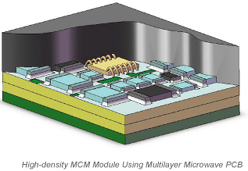 |
|||||||||
| About the invention patent | ||||||||||
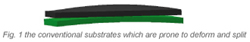
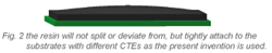
The present invention relates to a packaging method using resin to package bare chips or semiconductor components on organic substrates and composite dielectric substrates. The method is suitable for large scale, low cost and high yield packaging and is used in the packaging of electronic components, particularly in MCM and SIP packaging that widely used in communications, radar, navigation and home appliances. The present invention has conquered the difficulty that the conventional organic and composite dielectric substrates are prone to deform or split when being heated and can replace the expensive ceramic substrates widely used nowadays. |
||||||||||
| Technological innovations | ||||||||||
|
||||||||||
|
||||||||||
 |
 |
|||||||||
| Competitive edge & commercial values | ||||||||||
|
||||||||||
|
||||||||||
|
||||||||||
|
||||||||||
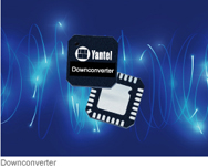
| The below RF microwave semiconductor products can be packaged when the present invention is used: | ||||||||||
|
||||||||||
 Look Shenzhen

 WeChat

 中文
中文