Microwave FET bias circuit
Time:2011-09-28
Publisher:admin
| Efficient and Lossless Temperature Compensation Bias Circuit Built-in GaAs FET Chip |
| US Utility Patented Technology(US7,420,420 B2) |
 |
|
|
| About the invention patent |
The present invention relates to a highly efficient and lossless temperature compensation circuit for RF FETs.
|
|
| Technological innovations |
|
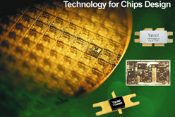
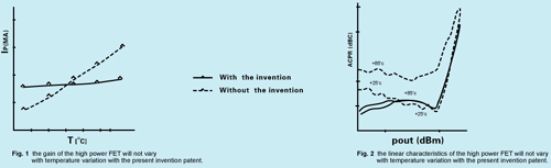
 The present circuit is particularly suitable for being packaged together witha high power FET into one GaAs chip. It is guaranteed that the gain and the linear characteristics of the high power FET will not vary with temperature variation by utilizing the present circuit to realize real-time tracking, controlling and compensatingthe static drain current of the high power FET. It can be used to design and manufacture RF power amplifier and oscillator. The present circuit is particularly suitable for being packaged together witha high power FET into one GaAs chip. It is guaranteed that the gain and the linear characteristics of the high power FET will not vary with temperature variation by utilizing the present circuit to realize real-time tracking, controlling and compensatingthe static drain current of the high power FET. It can be used to design and manufacture RF power amplifier and oscillator.
|
Meanwhile, with the present FET bias circuit, the difference of the static drain current of the high power FET fabricated in each chip at different positions in the whole wafer or batches of wafers will not be a problem. Thus, it can greatly increase the utilization factor of each wafer so that the cost is reduced.
|
 |
| Competitive edge & commercial values |
Currently, when manufacturing RF power amplifier, system manufacturers need to sort out FETs of close specifications for matching use and to design complicated peripheral circuits so as to realize the high efficient working and excellent linear characteristics of the high power FET. In addition, for semiconductor manufacturers, they need to waste partial chips so that the FETs can achieve high consistency to meet end-users’ requirement. To tackle the above two technological problems, global end-users need to consume expenditure up to billions of US dollars just to design and fabricate RF circuits, sort out and eliminate semiconductor chips. The present FET bias circuit can easily solve the two difficulties that have bothered RF design engineers all through.
|
The present circuit has the advantages of not increasing production procedures nor cost of chips, low cost, minimal power loss, high cost-performance, easy to be integrated and processed, particularly suitable for the design and fabrication of high power FET made of GaAs chips
|
The present invention is original in the world that it can realize lossless temperature compensation inside GaAs chips, be capable of keeping the gain and linearcharacteristics of the high power FET stable and not vary with temperature variation.
|
The present invention patent is the optimal solution for manufacturing high efficient RF FETs and RF power amplifiers.
|
 |
|

 Look Shenzhen

 WeChat

 中文
中文

